 | –≠–ª–µ–∫—Ç—Ä–æ–Ω–Ω—ã–π –∫–æ–º–ø–æ–Ω–µ–Ω—Ç: OPA2677 | –°–∫–∞—á–∞—Ç—å:  PDF PDF  ZIP ZIP |

THS6042, THS6043
350 mA,
±
12 V ADSL CPE LINE DRIVERS
SLOS264G ≠ MARCH 2000 ≠ REVISED DECEMBER 2001
1
POST OFFICE BOX 655303
∑
DALLAS, TEXAS 75265
D
Remote Terminal ADSL Line Driver
≠ Ideal for Both Full Rate ADSL and G.Lite
≠ Compatible With 1:1 Transformer Ratio
D
Low 2.1 pA/
Hz Noninverting Current Noise
≠ Reduces Noise Feedback Through
Hybrid Into Downstream Channel
D
Wide Supply Voltage Range
±
5 V to
±
15 V
≠ Ideal for
±
12-V Operation
D
Wide Output Swing
≠ 43-Vpp Differential Output Voltage,
R
L
= 200
,
±
12-V Supply
D
High Output Current
≠ 350 mA (typ)
D
High Speed
≠ 120 MHz (≠3 dB, G=1,
±
12 V, R
L
= 25
)
≠ 1200 V/
µ
s Slew Rate (G = 4,
±
12 V)
D
Low Distortion, Single-Ended, G = 4
≠ ≠79 dBc (250 kHz, 2 V
pp
, 100-
load)
D
Low Power Shutdown (THS6043)
≠ 300-
µ
A Total Standby Current
D
Thermal Shutdown and Short-Circuit
Protection
D
Standard SOIC, SOIC PowerPAD
and
TSSOP PowerPAD
Package
D
Evaluation Module Available
1
2
3
4
8
7
6
5
D1 OUT
D1 IN≠
D1 IN+
V
CC≠
V
CC+
D2 OUT
D2 IN≠
D2 IN+
THS6042
SOIC (D) AND
SOIC PowerPAD
(DDA) PACKAGE
(TOP VIEW)
1
2
3
4
5
6
7
14
13
12
11
10
9
8
D1 OUT
D1 IN≠
D1 IN+
V
CC≠
N/C
GND
N/C
V
CC+
D2 OUT
D2 IN≠
D2 IN+
N/C
SHUTDOWN
N/C
THS6043
SOIC (D) AND
TSSOP PowerPAD
(PWP) PACKAGE
(TOP VIEW)
description
The THS6042/3 is a high-speed line driver ideal for driving signals from the remote terminal to the central office
in asymmetrical digital subscriber line (ADSL) applications. It can operate from a
±
12-V supply voltage while
drawing only 8.2 mA of supply current per channel. It offers low ≠79 dBc total harmonic distortion driving a 100-
load (2 Vpp). The THS6042/3 offers a high 43-Vpp differential output swing across a 200-
load from a
±
12-V
supply. The THS6043 features a low-power shutdown mode, consuming only 300
µ
A quiescent current per
channel. The THS6042/3 is packaged in standard SOIC, SOIC PowerPAD, and TSSOP PowerPAD packages.
_
+
+12 V
750
VI+
_
+
≠12 V
750
VI≠
50
1:1
15.7 dBm
Delivered
to Telephone
Line
50
THS6042
Driver 1
THS6042
Driver 2
100
210
0.68
µ
F
RELATED PRODUCTS
DEVICE
THS6052/3
THS6092/3
OPA2677
THS6062
DESCRIPTION
175-mA,
±
12 ADSL CPE line driver
275-mA, +12 V ADSL CPE line driver
380-mA, +12 V ADSL CPE line driver
±
15 V to
±
5 V Low noise ADSL receiver
±
6 V to 5 V Low noise ADSL receiver
OPA2822
Copyright
2001, Texas Instruments Incorporated
PRODUCTION DATA information is current as of publication date.
Products conform to specifications per the terms of Texas Instruments
standard warranty. Production processing does not necessarily include
testing of all parameters.
Please be aware that an important notice concerning availability, standard warranty, and use in critical applications of
Texas Instruments semiconductor products and disclaimers thereto appears at the end of this data sheet.
PowerPAD is a trademark of Texas Instruments.

THS6042, THS6043
350 mA,
±
12 V ADSL CPE LINE DRIVERS
SLOS264G ≠ MARCH 2000 ≠ REVISED DECEMBER 2001
2
POST OFFICE BOX 655303
∑
DALLAS, TEXAS 75265
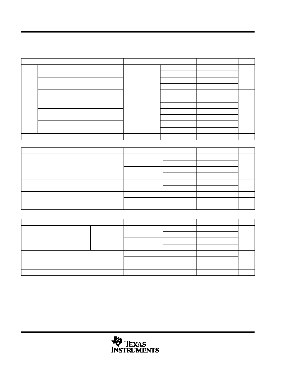
AVAILABLE OPTIONS
PACKAGED DEVICE
EVALUATION
TA
SOIC-8
(D)
SOIC-8 PowerPAD
(DDA)
SOIC-14
(D)
TSSOP-14
(PWP)
EVALUATION
MODULES
0
∞
C to 70
∞
C
THS6042CD
THS6042CDDA
THS6043CD
THS6043CPWP
THS6042EVM
THS6043EVM
≠ 40
∞
C to 85
∞
C
THS6042ID
THS6042IDDA
THS6043ID
THS6043IPWP
--
absolute maximum ratings over operating free-air temperature (unless otherwise noted)
Supply voltage, V
CC+
to V
CC≠
33
V
. . . . . . . . . . . . . . . . . . . . . . . . . . . . . . . . . . . . . . . . . . . . . . . . . . . . . . . . . . . . . . .
Input voltage
±
V
CC
. . . . . . . . . . . . . . . . . . . . . . . . . . . . . . . . . . . . . . . . . . . . . . . . . . . . . . . . . . . . . . . . . . . . . . . . . . . .
Output current (see Note 1)
450 mA
. . . . . . . . . . . . . . . . . . . . . . . . . . . . . . . . . . . . . . . . . . . . . . . . . . . . . . . . . . . . . .
Differential input voltage
±
4 V
. . . . . . . . . . . . . . . . . . . . . . . . . . . . . . . . . . . . . . . . . . . . . . . . . . . . . . . . . . . . . . . . . . .
Maximum junction temperature
150
∞
C
. . . . . . . . . . . . . . . . . . . . . . . . . . . . . . . . . . . . . . . . . . . . . . . . . . . . . . . . . . . .
Total power dissipation at (or below) 25
∞
C free-air temperature
See Dissipation Ratings Table
. . . . . . . . . . .
Operating free-air temperature, T
A
: Commercial 0
∞
C to 70
∞
C
. . . . . . . . . . . . . . . . . . . . . . . . . . . . . . . . . . . . . . . .
Industrial
≠ 40
∞
C to 85
∞
C
. . . . . . . . . . . . . . . . . . . . . . . . . . . . . . . . . . . . . . . .
Storage temperature, T
stg
: Commercial
≠ 65
∞
C to 125
∞
C
. . . . . . . . . . . . . . . . . . . . . . . . . . . . . . . . . . . . . . . . . . . .
Industrial
≠ 65
∞
C to 125
∞
C
. . . . . . . . . . . . . . . . . . . . . . . . . . . . . . . . . . . . . . . . . . . . . .
Lead temperature 1,6 mm (1/16 inch) from case for 10 seconds
300
∞
C
. . . . . . . . . . . . . . . . . . . . . . . . . . . . . . .
Stresses beyond those listed under "absolute maximum ratings" may cause permanent damage to the device. These are stress ratings only, and
functional operation of the device at these or any other conditions beyond those indicated under "recommended operating conditions" is not
implied. Exposure to absolute-maximum-rated conditions for extended periods may affect device reliability.
NOTE 1: The THS6042 and THS6043 may incorporate a PowerPAD on the underside of the chip. This acts as a heatsink and must be connected
to a thermally dissipating plane for proper power dissipation. Failure to do so may result in exceeding the maximum junction temperature
which could permanently damage the device. See TI Technical Brief SLMA002 for more information about utilizing the PowerPAD
thermally enhanced package.
DISSIPATION RATING TABLE
PACKAGE
JA
JC
TA = 25
∞
C
TJ = 150
∞
C
POWER RATING
D-8
95
∞
C/W
38.3
∞
C/W
1.32 W
DDA
45.8
∞
C/W
9.2
∞
C/W
2.73 W
D-14
66.6
∞
C/W
26.9
∞
C/W
1.88 W
PWP
37.5
∞
C/W
1.4
∞
C/W
3.3 W
This data was taken using the JEDEC proposed high-K test PCB. For the JEDEC low-K test
PCB, the
JA is168
∞
C/W for the D≠8 package and 122.3
∞
C/W for the D≠14 package.

THS6042, THS6043
350 mA,
±
12 V ADSL CPE LINE DRIVERS
SLOS264G ≠ MARCH 2000 ≠ REVISED DECEMBER 2001
3
POST OFFICE BOX 655303
∑
DALLAS, TEXAS 75265
recommended operating conditions
MIN
NOM
MAX
UNIT
Supply voltage V
to V
Dual supply
±
5
±
15
V
Supply voltage, VCC+ to VCC≠
Single supply
10
30
V
Operating free air temperature T
C-suffix
0
70
∞
C
Operating free-air temperature, TA
I-suffix
≠40
85
∞
C
electrical characteristics over recommended operating free-air temperature range, T
A
= 25
∞
C,
V
CC
=
±
12 V, R
(FEEDBACK)
= 750
, R
L
= 100
(unless otherwise noted)
dynamic performance
PARAMETER
TEST CONDITIONS
MIN
TYP
MAX
UNIT
G = 1, RF = 560
120
S
ll i
l b
d idth
RL = 25
G = 2, RF = 500
VCC =
±
6 V,
±
12 V
95
BW
Small-signal bandwidth
(≠ 3 dB)
L
G = 4, RF = 390
CC
75
MHz
(≠ 3 dB)
RL = 100
G = 4, RF = 390
VCC =
±
6 V
±
12 V
100
RL = 100
G = 8, RF = 280
VCC =
±
6 V,
±
12 V
65
G
2 R
390
VCC =
±
15 V
1000
RL = 25
G = 2, RF = 390
,
VO = 5 Vpp
VCC =
±
12 V
900
RL 25
VO = 5 Vpp
VCC =
±
6 V
600
SR
Slew rate (see Note 2)
G = 4, RF = 750
,
VCC =
±
15 V
1400
V/
µ
s
(
)
RL = 100
G = 4, RF = 750
,
VO = 12 Vpp
VCC =
±
12 V
1200
µ
RL = 100
G = 4, RF = 750
,
VO = 5 Vpp
VCC =
±
6 V
600
NOTE 2: Slew rate is defined from the 25% to the 75% output levels.
noise/distortion performance
PARAMETER
TEST CONDITIONS
MIN
TYP
MAX
UNIT
G = 4,
RL = 100
,
VO(pp) = 2 V
≠ 79
THD
Total harmonic distortion
(single-ended configuration)
G 4,
RL 100
,
VCC =
±
12 V, f = 250 kHz
VO(pp) = 16 V
≠ 75
dBc
THD
(single-ended configuration)
(RF = 390
)
G = 4,
RL = 25
,
VO(pp) = 2 V
≠ 72
dBc
(RF = 390
)
G 4,
RL 25
,
VCC =
±
6 V,
f = 250 kHz
VO(pp) = 7 V
≠ 68
Vn
Input voltage noise
VCC =
±
6 V,
±
12 V
f = 10 kHz
2.2
nV/
Hz
I
Input current noise
+Input
V
±
6 V
±
12 V
±
15 V
f
10 kHz
2.1
pA/
Hz
In
Input current noise
≠Input
VCC =
±
6 V,
±
12 V,
±
15 V
f = 10 kHz
11
pA/
Hz
Crosstalk
f = 250 kHz ,
VCC =
±
6 V,
±
12 V,
RF = 430
, RL = 100
V
2 Vpp G
4
≠ 71
dBc
Crosstalk
f = 250 kHz ,
VCC =
±
6 V,
±
12 V,
RF = 390
,
RL = 25
VO = 2 Vpp, G = 4
≠ 65
dBc
THS6042, THS6043
350 mA,
±
12 V ADSL CPE LINE DRIVERS
SLOS264G ≠ MARCH 2000 ≠ REVISED DECEMBER 2001
4
POST OFFICE BOX 655303
∑
DALLAS, TEXAS 75265
electrical characteristics over recommended operating free-air temperature range, T
A
= 25
∞
C,
V
CC
=
±
12 V, R
(FEEDBACK)
= 750
, R
L
= 100
(unless otherwise noted) (continued)
dc performance
PARAMETER
TEST CONDITIONS
MIN
TYP
MAX
UNIT
Input offset voltage
TA = 25
∞
C
9.5
16
Input offset voltage
TA = full range
21
mV
VOS
Differential offset voltage
VCC =
±
6 V,
±
12 V
TA = 25
∞
C
1
5
mV
VOS
Differential offset voltage
VCC
±
6 V,
±
12 V
TA = full range
7
Offset drift
TA = full range
20
µ
V/
∞
C
Input bias current
TA = 25
∞
C
3.5
10
≠ Input bias current
TA = full range
12
I
+ Input bias current
V
±
6 V
±
12 V
TA = 25
∞
C
1
5
A
IIB
+ Input bias current
VCC =
±
6 V,
±
12 V
TA = full range
6
µ
A
Differential input bias current
TA = 25
∞
C
3.5
10
Differential input bias current
TA = full range
12
ZOL
Open-loop transimpedance
RL = 1 k
VCC =
±
6 V,
±
12 V
1
M
input characteristics
PARAMETER
TEST CONDITIONS
MIN
TYP
MAX
UNIT
V
±
12 V
TA = 25
∞
C
±
9.6
±
10.1
V
Input common mode voltage range
VCC =
±
12 V
TA = full range
±
9.5
V
VICR
Input common-mode voltage range
V
±
6V
TA = 25
∞
C
±
3.7
±
4.2
V
VCC =
±
6V
TA = full range
±
3.6
CMRR
Common mode rejection ratio
V
±
6 V
±
12 V
TA = 25
∞
C
59
68
V
CMRR
Common-mode rejection ratio
VCC =
±
6 V,
±
12 V
TA = full range
55
V
R
Input resistance
+ Input
1.5
M
RI
Input resistance
≠ Input
15
Ci
Input capacitance
2
pF
output characteristics
PARAMETER
TEST CONDITIONS
MIN
TYP
MAX
UNIT
R
25
VCC =
±
12 V
±
7.5
±
9.1
V
Output voltage swing
Single ended
RL = 25
VCC =
±
6 V
±
4.1
±
4.6
V
VO
Output voltage swing
Single ended
100-mV overdrive
R
100
VCC =
±
12 V
±
10.3
±
10.8
V
RL = 100
VCC =
±
6 V
±
4.5
±
4.9
I
Output current
RL = 25
,
VCC =
±
12 V
300
350
mA
IO
Output current
RL = 10
,
VCC =
±
6 V
230
260
mA
IOS
Short-circuit current
RL = 0
,
VCC =
±
12 V
400
mA
ro
Output resistance
Open loop
15

THS6042, THS6043
350 mA,
±
12 V ADSL CPE LINE DRIVERS
SLOS264G ≠ MARCH 2000 ≠ REVISED DECEMBER 2001
5
POST OFFICE BOX 655303
∑
DALLAS, TEXAS 75265
electrical characteristics over recommended operating free-air temperature range, T
A
= 25
∞
C,
V
CC
=
±
12 V, R
(FEEDBACK)
= 750
, R
L
= 100
(unless otherwise noted) (continued)
power supply
PARAMETER
TEST CONDITIONS
MIN
TYP
MAX
UNIT
V
Operating range
Dual supply
±
4.5
±
16.5
V
VCC
Operating range
Single supply
9
33
V
V
±
12 V
TA = 25
∞
C
8.2
10.5
I
Quiescent current (each driver)
VCC =
±
12 V
TA = full range
11.5
mA
ICC
Quiescent current (each driver)
V
±
6 V
TA = 25
∞
C
7.4
9.5
mA
VCC =
±
6 V
TA = full range
10.5
V
±
12 V
TA = 25
∞
C
≠65
≠ 72
PSRR
Power supply rejection ratio
VCC =
±
12 V
TA = full range
≠62
dB
PSRR
Power supply rejection ratio
V
±
6 V
TA = 25
∞
C
≠62
≠ 69
dB
VCC =
±
6 V
TA = full range
≠60
shutdown characteristics (THS6043 only)
PARAMETER
TEST CONDITIONS
MIN
TYP
MAX
UNIT
VIL(SHDN)
Shutdown pin voltage for power up
VCC =
±
6 V,
±
12 V, GND = 0 V
(GND Pin as Reference)
0.8
V
VIH(SHDN)
Shutdown pin voltage for power down
VCC =
±
6 V,
±
12 V, GND = 0 V
(GND pin as reference)
2
V
ICC(SHDN) Total quiescent current when in shutdown state
VCC =
±
6 V,
±
12 V
0.3
0.7
mA
tDIS
Disable time (see Note 3)
VCC =
±
12 V
0.5
µ
s
tEN
Enable time (see Note 3)
VCC =
±
12 V
0.2
µ
s
IIL(SHDN)
Shutdown pin input bias current for power up
VCC =
±
6 V,
±
12 V
40
100
µ
A
IIH(SHDN)
Shutdown pin input bias current for power down
VCC =
±
6 V,
±
12 V V(SHDN) = 3.3 V
50
100
µ
A
NOTE 3: Disable/enable time is defined as the time from when the shutdown signal is applied to the SHDN pin to when the supply current has
reached half of its final value.

THS6042, THS6043
350 mA,
±
12 V ADSL CPE LINE DRIVERS
SLOS264G ≠ MARCH 2000 ≠ REVISED DECEMBER 2001
6
POST OFFICE BOX 655303
∑
DALLAS, TEXAS 75265
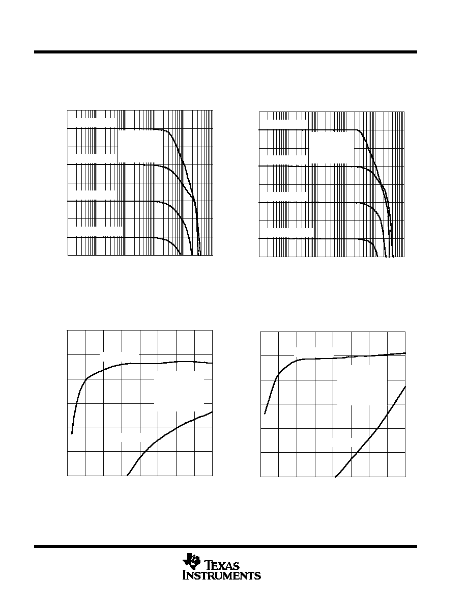
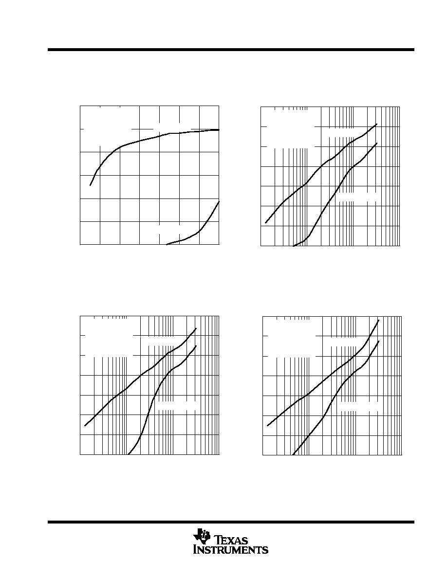
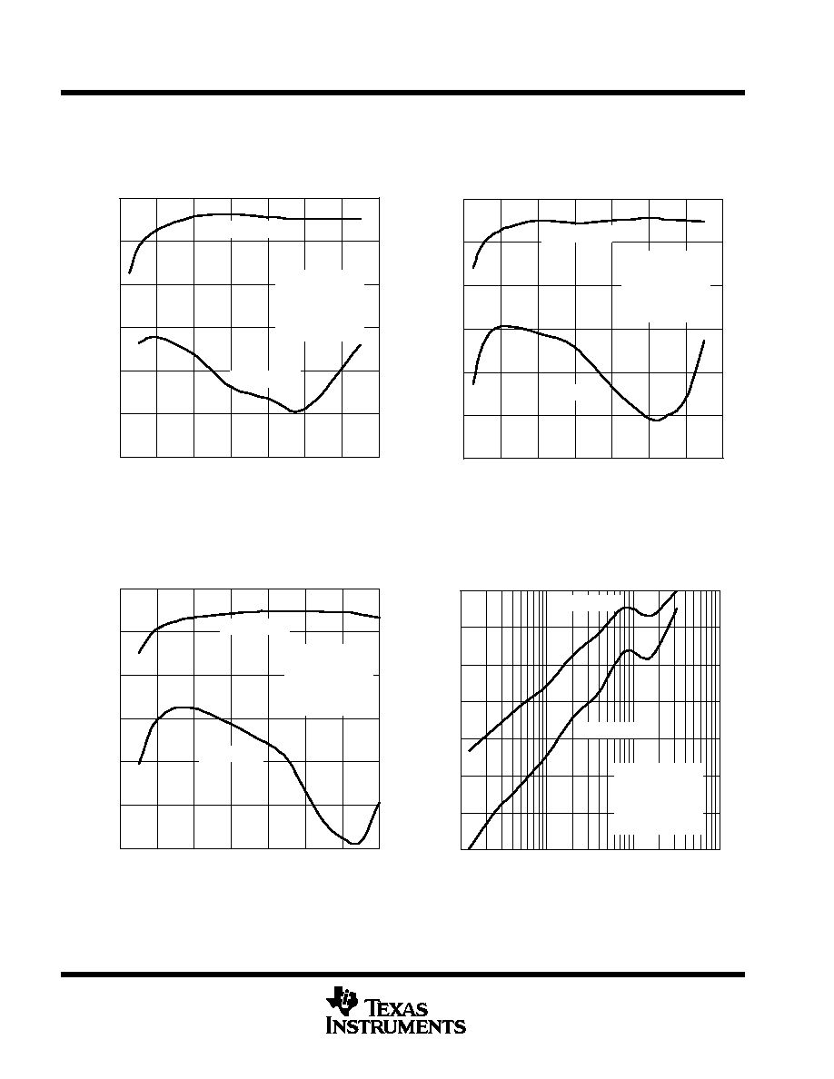
TYPICAL CHARACTERISTICS
Table of Graphs
FIGURE
Small and large signal output
vs Frequency
1 ≠ 6
Harmonic distortion
vs Output voltage
7, 8, 9
13, 14, 15
Harmonic distortion
vs Frequency
10, 11, 12,
16, 17, 18
Vn, In
Voltage noise and current noise
vs Frequency
19
Quiescent current
vs Free-air temperature
20
V
Positive output voltage headroom
vs Free-air temperature
21
V
Negative output voltage headroom
vs Free-air temperature
22
VO
Output voltage headroom
vs Output current
23
zo
Closed loop output impedance
vs Frequency
24
Quiescent current in shutdown mode
vs Free-air temperature
25
VIO
Input offset voltage and
differential input offset voltage
vs Free-air temperature
26
IIB
Input bias current
vs Free-air temperature
27
CMRR
Common-mode rejection ratio
vs Frequency
28
Crosstalk
vs Frequency
29
SR
Slew rate
vs Output voltage step
30
Shutdown response
31
Transimpedance and phase
vs Frequency
32
Overdrive recovery
33, 34
Small and large signal pulse response
35, 36

THS6042, THS6043
350 mA,
±
12 V ADSL CPE LINE DRIVERS
SLOS264G ≠ MARCH 2000 ≠ REVISED DECEMBER 2001
7
POST OFFICE BOX 655303
∑
DALLAS, TEXAS 75265
TYPICAL CHARACTERISTICS
Figure 1
≠24
≠18
≠12
≠6
0
6
12
18
24
10 K
100 K
1 M
10 M
100 M
1 G
VO = 8 VPP
VO = 2 VPP
VO = 0.5 VPP
VO = 0.125 VPP
f ≠ Frequency ≠ Hz
SMALL AND LARGE SIGNAL OUTPUT
vs
FREQUENCY
VCC =
±
12 V
G = 4
Rf = 750
RL = 100
Small and Large Signal Output
≠
dB
(V
PP
)
Figure 2
≠24
≠18
≠12
≠6
0
6
12
18
24
10 K
100 K
1 M
10 M
100 M
1 G
VO = 8 VPP
VO = 2 VPP
VO = 0.5 VPP
VO = 0.125 VPP
f ≠ Frequency ≠ Hz
SMALL AND LARGE SIGNAL OUTPUT
vs
FREQUENCY
VCC =
±
12 V
G = 4
Rf = 390
RL = 100
Small and Large Signal Output
≠
dB
(V
PP
)
Figure 3
≠18
≠12
≠6
0
6
12
18
24
30
10 K
100 K
1 M
10 M
100 M
1 G
VO = 16 VPP
VO = 4 VPP
VO = 1 VPP
VO = 0.25 VPP
f ≠ Frequency ≠ Hz
SMALL AND LARGE SIGNAL OUTPUT
vs
FREQUENCY
VCC =
±
12 V
G = 8
Rf = 280
RL = 100
Small and Large Signal Output
≠
dB
(V
PP
)
Figure 4
≠18
≠12
≠6
0
6
12
18
24
30
10 K
100 K
1 M
10 M
100 M
1 G
VO = 16 VPP
VO = 4 VPP
VO = 1 VPP
VO = 0.25 VPP
f ≠ Frequency ≠ Hz
SMALL AND LARGE SIGNAL OUTPUT
vs
FREQUENCY
VCC =
±
12 V
G = 8
Rf = 750
RL = 100
Small and Large Signal Output
≠
dB
(V
PP
)
THS6042, THS6043
350 mA,
±
12 V ADSL CPE LINE DRIVERS
SLOS264G ≠ MARCH 2000 ≠ REVISED DECEMBER 2001
8
POST OFFICE BOX 655303
∑
DALLAS, TEXAS 75265
TYPICAL CHARACTERISTICS
Figure 5
≠24
≠18
≠12
≠6
0
6
12
18
24
10 K
100 K
1 M
10 M
100 M
1 G
VO = 8 VPP
VO = 2 VPP
VO = 0.5 VPP
VO = 0.125 VPP
f ≠ Frequency ≠ Hz
SMALL AND LARGE SIGNAL OUTPUT
vs
FREQUENCY
VCC =
±
6 V
G = 4
Rf = 750
RL = 25
Small and Large Signal Output
≠
dB
(V
PP
)
Figure 6
≠24
≠18
≠12
≠6
0
6
12
18
24
10 K
100 K
1 M
10 M
100 M
1 G
VO = 8 VPP
VO = 2 VPP
VO = 0.5 VPP
VO = 0.125 VPP
f ≠ Frequency ≠ Hz
SMALL AND LARGE SIGNAL OUTPUT
vs
FREQUENCY
VCC =
±
6 V
G = 4
Rf = 390
RL = 25
Small and Large Signal Output
≠
dB
(V
PP
)
Figure 7
≠100
≠95
≠90
≠85
≠80
≠75
≠70
0
2
4
6
8
10
12
14
16
Harmonic Distortion
≠
dBc
HARMONIC DISTORTION
vs
OUTPUT VOLTAGE
VO ≠ Output Voltage ≠ VPP
VCC =
±
15 V
Gain = 4
RL = 100
Rf = 390
f = 250 KHz
2nd Order
3rd Order
Figure 8
≠100
≠95
≠90
≠85
≠80
≠75
≠70
0
2
4
6
8
10
12
14
16
Harmonic Distortion
≠
dBc
HARMONIC DISTORTION
vs
OUTPUT VOLTAGE
VO ≠ Output Voltage ≠ VPP
VCC =
±
10 V
Gain = 4
RL = 100
Rf = 390
f = 250 KHz
2nd Order
3rd Order
THS6042, THS6043
350 mA,
±
12 V ADSL CPE LINE DRIVERS
SLOS264G ≠ MARCH 2000 ≠ REVISED DECEMBER 2001
9
POST OFFICE BOX 655303
∑
DALLAS, TEXAS 75265
TYPICAL CHARACTERISTICS
Figure 9
≠100
≠95
≠90
≠85
≠80
≠75
≠70
0
1
2
3
4
5
6
7
Harmonic Distortion
≠
dBc
HARMONIC DISTORTION
vs
OUTPUT VOLTAGE
VO ≠ Output Voltage ≠ VPP
VCC =
±
5.4 V
Gain = 4
RL = 100
Rf = 390
f = 250 KHz
2nd Order
3rd Order
Figure 10
≠100
≠90
≠80
≠70
≠60
≠50
≠40
≠30
100 k
1 M
10 M
100 M
Harmonic Distortion
≠
dBc
HARMONIC DISTORTION
vs
FREQUENCY
VCC =
±
15 V
Gain = 4
RL = 100
Rf = 390
VO = 2 VPP
2nd Order
3rd Order
f ≠ Frequency ≠ Hz
Figure 11
≠100
≠90
≠80
≠70
≠60
≠50
≠40
≠30
100 k
1 M
10 M
100 M
Harmonic Distortion
≠
dBc
HARMONIC DISTORTION
vs
FREQUENCY
VCC =
±
10 V
Gain = 4
RL = 100
Rf = 390
VO = 2 VPP
2nd Order
3rd Order
f ≠ Frequency ≠ Hz
Figure 12
≠100
≠90
≠80
≠70
≠60
≠50
≠40
≠30
100 k
1 M
10 M
100 M
Harmonic Distortion
≠
dBc
HARMONIC DISTORTION
vs
FREQUENCY
VCC =
±
5.4 V
Gain = 4
RL = 100
Rf = 390
VO = 2 VPP
2nd Order
3rd Order
f ≠ Frequency ≠ Hz
THS6042, THS6043
350 mA,
±
12 V ADSL CPE LINE DRIVERS
SLOS264G ≠ MARCH 2000 ≠ REVISED DECEMBER 2001
10
POST OFFICE BOX 655303
∑
DALLAS, TEXAS 75265
TYPICAL CHARACTERISTICS
Figure 13
≠100
≠95
≠90
≠85
≠80
≠75
≠70
0
2
4
6
8
10
12
14
Harmonic Distortion
≠
dBc
HARMONIC DISTORTION
vs
OUTPUT VOLTAGE
VO ≠ Output Voltage ≠ VPP
VCC =
±
15 V
Gain = 4
RL = 25
Rf = 390
f = 250 KHz
2nd Order
3rd Order
Figure 14
≠100
≠95
≠90
≠85
≠80
≠75
≠70
0
2
4
6
8
10
12
14
Harmonic Distortion
≠
dBc
HARMONIC DISTORTION
vs
OUTPUT VOLTAGE
VO ≠ Output Voltage ≠ VPP
VCC =
±
10 V
Gain = 4
RL = 25
Rf = 390
f = 250 KHz
2nd Order
3rd Order
Figure 15
≠100
≠95
≠90
≠85
≠80
≠75
≠70
0
1
2
3
4
5
6
7
Harmonic Distortion
≠
dBc
HARMONIC DISTORTION
vs
OUTPUT VOLTAGE
VO ≠ Output Voltage ≠ VPP
VCC =
±
5.4 V
Gain = 4
RL = 25
Rf = 390
f = 250 KHz
2nd Order
3rd Order
Figure 16
≠100
≠90
≠80
≠70
≠60
≠50
≠40
≠30
100 k
1 M
10 M
100 M
Harmonic Distortion
≠
dBc
HARMONIC DISTORTION
vs
FREQUENCY
VCC =
±
15 V
Gain = 4
RL = 25
Rf = 390
VO = 2 VPP
2nd Order
3rd Order
f ≠ Frequency ≠ Hz

THS6042, THS6043
350 mA,
±
12 V ADSL CPE LINE DRIVERS
SLOS264G ≠ MARCH 2000 ≠ REVISED DECEMBER 2001
11
POST OFFICE BOX 655303
∑
DALLAS, TEXAS 75265
TYPICAL CHARACTERISTICS
Figure 17
≠100
≠90
≠80
≠70
≠60
≠50
≠40
≠30
100 k
1 M
10 M
100 M
Harmonic Distortion
≠
dBc
HARMONIC DISTORTION
vs
FREQUENCY
VCC =
±
10 V
Gain = 4
RL = 25
Rf = 390
VO = 2 VPP
2nd Order
3rd Order
f ≠ Frequency ≠ Hz
Figure 18
≠100
≠90
≠80
≠70
≠60
≠50
≠40
≠30
100 k
1 M
10 M
100 M
Harmonic Distortion
≠
dBc
HARMONIC DISTORTION
vs
FREQUENCY
VCC =
±
5.4 V
Gain = 4
RL = 25
Rf = 390
VO = 2 VPP
2nd Order
3rd Order
f ≠ Frequency ≠ Hz
Figure 19
1
10
100
10
100
1 k
10 k
100 k
IN+
IN≠
Vn
nV/
Hz
≠
V
oltage
Noise
≠
V
n
I n
≠
Current Noise
≠
pA/
Hz
VOLTAGE NOISE AND CURRENT NOISE
vs
FREQUENCY
f ≠ Frequency ≠ Hz
VCC =
±
5 V to
±
15 V
TA = 25
∞
C
Figure 20
5.5
6
6.5
7
7.5
8
8.5
9
9.5
10
≠40
≠20
0
20
40
60
80
100
VCC =
±
12 V
VCC =
±
6 V
Quiescent Current
≠
mA
QUIESCENT CURRENT
vs
FREE-AIR TEMPERATURE
TA ≠ Free-Air Temperature ≠
∞
C
Per Amplifier

THS6042, THS6043
350 mA,
±
12 V ADSL CPE LINE DRIVERS
SLOS264G ≠ MARCH 2000 ≠ REVISED DECEMBER 2001
12
POST OFFICE BOX 655303
∑
DALLAS, TEXAS 75265
TYPICAL CHARACTERISTICS
Figure 21
1.05
1.1
1.15
1.2
1.25
1.3
1.35
≠40
≠20
0
20
40
60
80
100
VCC =
±
6 V, RL = 25
VCC =
±
12 V, RL = 100
VCC =
±
6 V, RL = 100
Positive Output V
oltage Headroom
≠
V
POSITIVE OUTPUT VOLTAGE HEADROOM
vs
FREE-AIR TEMPERATURE
TA ≠ Free-Air Temperature ≠
∞
C
(+VCC ≠ VO)
Figure 22
≠1.35
≠1.3
≠1.25
≠1.2
≠1.15
≠1.1
≠1.05
≠40
≠20
0
20
40
60
80
100
VCC =
±
12 V, RL = 100
VCC =
±
6 V, RL = 25
NEGATIVE OUTPUT VOLTAGE HEADROOM
vs
FREE-AIR TEMPERATURE
TA ≠ Free-Air Temperature ≠
∞
C
VCC =
±
6 V, RL = 100
Negative Output V
oltage Headroom
≠
V
(≠VCC ≠ VO)
Figure 23
1
1.5
2
2.5
3
3.5
4
0
100
200
300
400
500
Output V
oltage Headroom
≠
| V |
OUTPUT VOLTAGE HEADROOM
vs
OUTPUT CURRENT
IO ≠ Output Current ≠ | mA |
| VCC | ≠ | VO |
VCC =
±
12 V and
±
6 V
0.01
0.1
1
10
100
100 K
1 M
10 M
100 M
1 G
f ≠ Frequency ≠ Hz
≠
Closed Loop Output Impedance
≠
Z
o
CLOSED LOOP OUTPUT IMPEDANCE
vs
FREQUENCY
Gain = 8
Gain = 4
Gain = 2
VCC =
±
5 V to
±
15 V
RL = 100
Rf = 750
Figure 24
THS6042, THS6043
350 mA,
±
12 V ADSL CPE LINE DRIVERS
SLOS264G ≠ MARCH 2000 ≠ REVISED DECEMBER 2001
13
POST OFFICE BOX 655303
∑
DALLAS, TEXAS 75265
TYPICAL CHARACTERISTICS
Figure 25
TA ≠ Free-Air Temperature ≠
∞
C
0.15
0.2
0.25
0.3
0.35
0.4
≠40
≠20
0
20
40
60
80
100
Quiscent Current In Shutdown Mode
≠
QUIESCENT CURRENT IN SHUTDOWN MODE
vs
FREE-AIR TEMPERATURE
A
µ
VCC =
±
12 V
VCC =
±
6 V
Both Amplifiers
Figure 26
7
8
9
10
11
12
≠40
≠20
0
20
40
60
80
100
0
0.1
0.2
0.3
0.4
0.5
VOS
Differential VOS
VCC =
±
6 V to
±
12 V
≠
Input Offset V
oltage
≠
mV
INPUT OFFSET VOLTAGE AND
DIFFERENTIAL INPUT OFFSET VOLTAGE
vs
FREE-AIR TEMPERATURE
V
IO
TA ≠ Temperature ≠
∞
C
Differential Input Offset V
oltage
≠
mV
Figure 27
0
0.5
1
1.5
2
2.5
3
3.5
4
4.5
5
≠40
≠20
0
20
40
60
80
100
≠
Input Bias Current
≠
INPUT BIAS CURRENT
vs
FREE-AIR TEMPERATURE
I IB
A
µ
TA ≠ Temperature ≠
∞
C
VCC =
±
6 V to
±
12 V
IIB≠
IIB+
20
30
40
50
60
70
80
10 k
100 k
1 M
10 M
100 M
Gain = 2
Rf = 1 k
VCC = +6 V
RL = 25
VCC = +12 V
RL = 100
CMRR
≠
Common-Mode Rejection Ratio
≠
dB
f ≠ Frequency ≠ Hz
COMMON-MODE REJECTION RATIO
vs
FREQUENCY
Figure 28

THS6042, THS6043
350 mA,
±
12 V ADSL CPE LINE DRIVERS
SLOS264G ≠ MARCH 2000 ≠ REVISED DECEMBER 2001
14
POST OFFICE BOX 655303
∑
DALLAS, TEXAS 75265
TYPICAL CHARACTERISTICS
≠90
≠80
≠70
≠60
≠50
≠40
≠30
≠20
≠10
0
100 k
1 M
10 M
100 M
Rf = 390
RL = 25
Rf = 430
RL = 100
VCC =
±
6 V to
±
12 V
Gain = 4
Crosstalk
≠
dB
CROSSTALK
vs
FREQUENCY
f ≠ Frequency ≠ Hz
Figure 29
Figure 30
0
200
400
600
800
1000
1200
1400
1600
1800
0
2
4
6
8
10
12
14
16
SR
≠
Slew Rate
≠
Output Voltage Step ≠ V
SLEW RATE
vs
OUTPUT VOLTAGE STEP
s
µ
V/
VCC =
±
15 V
VCC =
±
12 V
VCC =
±
6 V
Gain = 4
RL = 100
Rf = 750
Figure 31
≠1
0
1
2
3
4
5
6
7
0
4
8
12
16
20
≠13
≠11
≠9
≠7
≠5
≠3
≠1
1
3
≠
Output V
oltage
≠
V
SHUTDOWN RESPONSE
V
O
t ≠ Time ≠
µ
s
VO
V(SHDN)
Shutdown Pin V
oltage
≠
V
Gain = 8
VCC +12 V
Rf = 750
RL = 100
20
40
60
80
100
120
140
1 K
10 K
100 K
1 M
10 M
100 M
1 G
≠225
≠180
≠135
≠90
≠45
0
45
T
ransimpedance
≠
dB
f ≠ Frequency ≠ Hz
TRANSIMPEDANCE AND PHASE
vs
FREQUENCY
VCC =
±
5 V to
±
15 V
RL = 1 k
Phase
≠
Degrees
Figure 32
Phase
Transimpedance
THS6042, THS6043
350 mA,
±
12 V ADSL CPE LINE DRIVERS
SLOS264G ≠ MARCH 2000 ≠ REVISED DECEMBER 2001
15
POST OFFICE BOX 655303
∑
DALLAS, TEXAS 75265
TYPICAL CHARACTERISTICS
≠16
≠12
≠8
≠4
0
4
8
12
16
0
40
80
120
160
200
≠2
≠1.5
≠1
≠0.5
0
0.5
1
1.5
2
VI
VO
≠
Output V
oltage
≠
V
t ≠ Time ≠ ns
OVERDRIVE RECOVERY
≠
Input
V
oltage
≠
V
V
O
V
I
Gain = ≠8
VCC =
±
12 V
Rf = 750
RL = 100
Figure 33
Figure 34
≠16
≠12
≠8
≠4
0
4
8
12
16
0
40
80
120
160
200
≠2
≠1.5
≠1
≠0.5
0
0.5
1
1.5
2
VO
≠
Output V
oltage
≠
V
t ≠ Time ≠ ns
OVERDRIVE RECOVERY
≠
Input V
oltage
≠
V
V
O
V
I
Gain = 8
VCC =
±
12 V
Rf = 750
RL = 100
VI
Figure 35
≠0.6
≠0.4
≠0.2
0
0.2
0.4
0.6
0
40
80
120
160
200
≠6
≠4
≠2
0
2
4
6
Small Signal Output
≠
V
t ≠ Time ≠ ns
SMALL AND LARGE SIGNAL PULSE RESPONSE
Large Signal Output
≠
V
Small Signal
Large Signal
Gain = ≠8
VCC =
±
12 V
Rf = 750
RL = 100
Figure 36
≠0.6
≠0.4
≠0.2
0
0.2
0.4
0.6
0
40
80
120
160
200
≠6
≠4
≠2
0
2
4
6
Small Signal Output
≠
V
t ≠ Time ≠ ns
SMALL AND LARGE SIGNAL PULSE RESPONSE
Large Signal Output
≠
V
Gain = 8
VCC =
±
12 V
Rf = 750
RL = 100
Small Signal
Large Signal

THS6042, THS6043
350 mA,
±
12 V ADSL CPE LINE DRIVERS
SLOS264G ≠ MARCH 2000 ≠ REVISED DECEMBER 2001
16
POST OFFICE BOX 655303
∑
DALLAS, TEXAS 75265
APPLICATION INFORMATION
The THS6042/3 contain two independent operational amplifiers. These amplifiers are current feedback
topology amplifiers made for high-speed operation. They have been specifically designed to deliver the full
power requirements of ADSL and therefore can deliver output currents of at least 230 mA at full output voltage.
The THS6042/3 are fabricated using the Texas Instruments 30-V complementary bipolar process, HVBiCOM.
This process provides excellent isolation and high slew rates that result in the device's excellent crosstalk and
extremely low distortion.
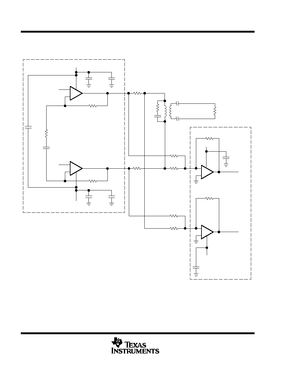
ADSL
The THS6042/3 were primarily designed as line drivers for ADSL (asymmetrical digital subscriber line). The
driver output stage has been sized to provide full ADSL power levels of 13 dBm onto the telephone lines.
Although actual driver output peak voltages and currents vary with each particular ADSL application, the
THS6042/3 are specified for a minimum full output current of 230 mA at
±
6 V and 300 mA at the full output
voltage of
±
12 V. This performance meets the demanding needs of ADSL at the client side end of the telephone
line. A typical ADSL schematic is shown in Figure 37.
The ADSL transmit band consists of 255 separate carrier frequencies each with its own modulation and
amplitude level. With such an implementation, it is imperative that signals put onto the telephone line have as
low a distortion as possible. This is because any distortion either interferes directly with other ADSL carrier
frequencies or creates intermodulation products that interfere with other ADSL carrier frequencies.
The THS6042/3 have been specifically designed for ultra low distortion by careful circuit implementation and
by taking advantage of the superb characteristics of the complementary bipolar process. Driver single-ended
distortion measurements are shown in Figures 7 ≠ 15. In the differential driver configuration, the second order
harmonics tend to cancel out. Thus, the dominant total harmonic distortion (THD) is primarily due to the third
order harmonics. Additionally, distortion should be reduced as the feedback resistance drops. This is because
the bandwidth of the amplifier increases, which allows the amplifier to react faster to any nonlinearities in the
closed-loop system. Another significant point is the fact that distortion decreases as the impedance load
increases. This is because the output resistance of the amplifier becomes less significant as compared to the
output load resistance.
Even though the THS6042/3 are designed to drive ADSL signals that have a maximum bandwidth of 1.1 MHz,
reactive loading from the transformer can cause some serious issues. Most transformers have a resonance
peak typically occurring from 20 MHz up to 150 MHz depending on the manufacturer and construction
technique. This resonance peak can cause some serious issues with the line driver amplifier such as small
high-frequency oscillations, increased current consumption, and/or ringing. Although the series termination
resistor helps isolate the transformer's resonance from the line-driver amplifier, additional means may be
necessary to eliminate the effects of a reactive load. The simplest way is to add a snubber network, also known
as a zoebel network, in parallel with the transformer as shown by R
(SNUB)
and C
(SNUB)
in Figure 36. At high
frequencies, where the transformer's impedance becomes very high at its resonance frequency (ex: 1 k
@
100 MHz), the snubber provides a resistive load to the circuit. The value for R
(SNUB)
should initially be set to
the impedance presented by the transformer within its pass-band. An example of this would be to use a 100-
resistor for a 1:1 transformer or a 25-
resistor for a 1:2 transformer. The value for C
(SNUB)
should be chosen
such that the ≠3 dB frequency is about 5 times less than the resonance frequency. For example,if the resonance
frequency is at 100 MHz, the impedance of C
(SNUB)
should be equal to R
(SNUB)
at 20 MHz. This leads to a value
of C
(SNUB)
= 1 / (2
f R
(SNUB)
), or approximately 82 pF. This should only be used as a starting point. The final
values will be dictated by actual circuit testing.
THS6042, THS6043
350 mA,
±
12 V ADSL CPE LINE DRIVERS
SLOS264G ≠ MARCH 2000 ≠ REVISED DECEMBER 2001
17
POST OFFICE BOX 655303
∑
DALLAS, TEXAS 75265
APPLICATION INFORMATION
ADSL (continued)
One problem in the ADSL CPE area is noise. It is imperative that signals received off the telephone line have
as high a signal-to-noise ratio (SNR) as possible. This is because of the numerous sources of interference on
the line. The best way to accomplish this high SNR is to have a low-noise receiver such as the THS6062 or
OPA2822 on the front-end. Even if the receiver has very low noise characteristics, noise could be dominated
by the line driver amplifier. The THS6042/3 were primarily designed to circumvent this issue.
The ADSL standard, ANSI T1.413, stipulates a noise power spectral density of ≠140 dBm/Hz, which is
equivalent to 31.6 nV/
Hz for a 100-
system. Although many amplifiers can reach this level of performance,
actual ADSL system testing has indicated that the noise power spectral density may be required to have
≠150
dBm/Hz, or
10 nV/
Hz. With a transformer ratio of 1:2, this number reduces to less than 5 nV/
Hz. The
THS6042/3, with an equivalent input noise of 2.2 nV/
Hz, is an excellent choice for this application. Coupled
with a low 2.1 pA/
Hz noninverting current noise, a very low 11 pA/
Hz inverting current noise, and low value
resistors, the THS6042/3 ensures that the received signal SNR is as high as possible.
THS6042, THS6043
350 mA,
±
12 V ADSL CPE LINE DRIVERS
SLOS264G ≠ MARCH 2000 ≠ REVISED DECEMBER 2001
18
POST OFFICE BOX 655303
∑
DALLAS, TEXAS 75265
APPLICATION INFORMATION
ADSL (continued)
_
+
10
µ
F
0.1
µ
F
+12 V
750
+
VI+
_
+
10
µ
F
0.1
µ
F
≠12 V
750
+
VI≠
+
≠
499
0.1
µ
F
499
1 k
50
+
≠
499
499
1 k
1:1
Telephone Line
50
+12 V
≠12 V
0.1
µ
F
THS6062
Receiver 1
THS6062
Receiver 2
VO+
VO≠
THS6042
Driver 1
THS6042
Driver 2
100
210
1
µ
F
0.68
µ
F
R(SNUB)
C(SNUB)
Figure 37. THS6042 ADSL Application With 1:1 Transformer Ratio

THS6042, THS6043
350 mA,
±
12 V ADSL CPE LINE DRIVERS
SLOS264G ≠ MARCH 2000 ≠ REVISED DECEMBER 2001
19
POST OFFICE BOX 655303
∑
DALLAS, TEXAS 75265
APPLICATION INFORMATION
noise calculations and noise figure
Noise can cause errors on very small signals. This is especially true for the amplifying small signals. The noise
model for current feedback amplifiers (CFB) is the same as voltage feedback amplifiers (VFB). The only
difference between the two is that the CFB amplifiers generally specify different current noise parameters for
each input, while VFB amplifiers usually only specify one noise current parameter. The noise model is shown
in Figure 38. This model includes all of the noise sources as follows:
∑
e
n
= Amplifier internal voltage noise (nV/
Hz)
∑
IN+ = Noninverting current noise (pA/
Hz)
∑
IN≠ = Inverting current noise (pA/
Hz)
∑
e
Rx
= Thermal voltage noise associated with each resistor (e
Rx
= 4 kTR
x
)
_
+
RF
RS
RG
eRg
eRf
eRs
en
IN+
Noiseless
IN≠
eni
eno
Figure 38. Noise Model
The total equivalent input noise density (e
ni
) is calculated by using the following equation:
e
ni
+
en
2
)
IN
)
R
S
2
)
IN≠
R
F
¯
R
G
2
)
4 kTRs
)
4 kT R
F
¯
R
G
Where:
k = Boltzmann's constant = 1.380658
◊
10
≠23
T = Temperature in degrees Kelvin (273 +
∞
C)
R
F
|| R
G
= Parallel resistance of R
F
and R
G
To get the equivalent output noise of the amplifier, just multiply the equivalent input noise density (e
ni
) by the
overall amplifier gain (A
V
).
eno
+
e
ni
A
V
+
e
ni
1
)
R
F
R
G
(Noninverting Case)
As the previous equations show, to keep noise at a minimum, small value resistors should be used. As the
closed-loop gain is increased (by reducing R
G
), the input noise is reduced considerably because of the parallel
resistance term. This leads to the general conclusion that the most dominant noise sources are the source
resistor (R
S
) and the internal amplifier noise voltage (e
n
). Because noise is summed in a root-mean-squares
method, noise sources smaller than 25% of the largest noise source can be effectively ignored. This can greatly
simplify the formula and make noise calculations much easier to calculate.
THS6042, THS6043
350 mA,
±
12 V ADSL CPE LINE DRIVERS
SLOS264G ≠ MARCH 2000 ≠ REVISED DECEMBER 2001
20
POST OFFICE BOX 655303
∑
DALLAS, TEXAS 75265
APPLICATION INFORMATION
noise calculations and noise figure (continued)
This brings up another noise measurement usually preferred in RF applications, the noise figure (NF). Noise
figure is a measure of noise degradation caused by the amplifier. The value of the source resistance must be
defined and is typically 50
in RF applications.
NF
+
10log
e
2
ni
e
Rs
2
Because the dominant noise components are generally the source resistance and the internal amplifier noise
voltage, we can approximate noise figure as:
NF
+
10log 1
)
e
n
2
)
IN
)
R
S
2
4 kTR
S
Figure 39 shows the noise figure graph for the THS6042/3.
0
2
4
6
8
10
12
14
16
10
100
1 k
10 k
Noise Figure
≠
dB
RS ≠ Source Resistance ≠
f = 10 kHz
TA = 25
∞
C
Figure 39. Noise Figure vs Source Resistance

THS6042, THS6043
350 mA,
±
12 V ADSL CPE LINE DRIVERS
SLOS264G ≠ MARCH 2000 ≠ REVISED DECEMBER 2001
21
POST OFFICE BOX 655303
∑
DALLAS, TEXAS 75265
APPLICATION INFORMATION
device protection features
The THS6042/3 have two built-in features that protect the devices against improper operation. The first
protection mechanism is output current limiting. Should the output become shorted to ground, the output current
is automatically limited to the value given in the data sheet. While this protects the output against excessive
current, the device internal power dissipation increases due to the high current and large voltage drop across
the output transistors. Continuous output shorts are not recommended and could damage the device.
The second built-in protection feature is thermal shutdown. Should the internal junction temperature rise above
approximately 180
_
C, the device automatically shuts down. Such a condition could exist with improper heat
sinking or if the output is shorted to ground. When the abnormal condition is fixed, the internal thermal shutdown
circuit automatically turns the device back on.
thermal information ≠ PowerPAD
The THS6042/3 are available packaged in thermally-enhanced PowerPAD packages. These packages are
constructed using a downset leadframe upon which the die is mounted [see Figure 40(a) and Figure 40(b)]. This
arrangement results in the lead frame being exposed as a thermal pad on the underside of the package [see
Figure 40(c)]. Because this thermal pad has direct thermal contact with the die, excellent thermal performance
can be achieved by providing a good thermal path away from the thermal pad.
The PowerPAD package allows for both assembly and thermal management in one manufacturing operation.
During the surface-mount solder operation (when the leads are being soldered), the thermal pad can also be
soldered to a copper area underneath the package. Through the use of thermal paths within this copper area,
heat can be conducted away from the package into either a ground plane or other heat dissipating device. This
is discussed in more detail in the PCB design considerations section of this document.
The PowerPAD package represents a breakthrough in combining the small area and ease of assembly of
surface mount with the, heretofore, awkward mechanical methods of heatsinking.
DIE
Side View (a)
End View (b)
Bottom View (c)
DIE
Thermal
Pad
NOTE A: The thermal pad is electrically isolated from all terminals in the package.
Figure 40. Views of Thermally Enhanced PWP Package

THS6042, THS6043
350 mA,
±
12 V ADSL CPE LINE DRIVERS
SLOS264G ≠ MARCH 2000 ≠ REVISED DECEMBER 2001
22
POST OFFICE BOX 655303
∑
DALLAS, TEXAS 75265
APPLICATION INFORMATION
PCB design considerations
Proper PCB design techniques in two areas are important to assure proper operation of the THS6042/3. These
areas are high-speed layout techniques and thermal-management techniques. Because the devices are
high-speed parts, the following guidelines are recommended.
D
Ground plane ≠ It is essential that a ground plane be used on the board to provide all components with a
low inductive ground connection. Although a ground connection directly to a terminal of the THS6042/3 is
not necessarily required, it is highly recommended that the thermal pad of the package be tied to ground.
This serves two functions. It provides a low inductive ground to the device substrate to minimize internal
crosstalk and it provides the path for heat removal.
D
Input stray capacitance ≠ To minimize potential problems with amplifier oscillation, the capacitance at the
inverting input of the amplifiers must be kept to a minimum. To do this, PCB trace runs to the inverting input
must be as short as possible, the ground plane must be removed under any etch runs connected to the
inverting input, and external components should be placed as close as possible to the inverting input. This
is especially true in the noninverting configuration. An example of this can be seen in Figure 41, which shows
what happens when a 2.2-pF capacitor is added to the inverting input terminal in the noninverting
configuration. The bandwidth increases dramatically at the expense of peaking. This is because some of
the error current is flowing through the stray capacitor instead of the inverting node of the amplifier. While
the device is in the inverting mode, stray capacitance at the inverting input has a minimal effect. This is
because the inverting node is at a virtual ground and the voltage does not fluctuate nearly as much as in
the noninverting configuration. This can be seen in Figure 42, where a 22-pF capacitor adds only 0.9 dB
of peaking. In general, as the gain of the system increases, the output peaking due to this capacitor
decreases. While this can initally appear to be a faster and better system, overshoot and ringing are more
likely to occur under fast transient conditions. So, proper analysis of adding a capacitor to the inverting input
node should always be performed for stable operation.
Figure 41
≠10
≠8
≠6
≠4
≠2
0
2
4
6
750
C in
VI
+
≠
VO
50
50
100 k
OUTPUT AMPLITUDE
vs
FREQUENCY
1 G
f ≠ Frequency ≠ Hz
1 M
10 M
100 M
Output Amplitude
≠
dB
VCC =
±
12 V
Gain = 1
RL = 50
VO = 0.1 V
Ci = 0 pF
(Stray C Only)
Ci = 2.2 pF
Figure 42
≠7
≠6
≠5
≠4
≠3
≠2
≠1
0
1
2
100 k
OUTPUT AMPLITUDE
vs
FREQUENCY
1 G
f ≠ Frequency ≠ Hz
1 M
10 M
100 M
Output Amplitude
≠
dB
750
C in
VI
+
≠
VO
RL = 50
50
Rg
Ci = 0 pF
(Stray C Only)
Ci = 22 pF
VCC =
±
12 V
Gain = ≠1
RL = 50
VO = 0.1 V

THS6042, THS6043
350 mA,
±
12 V ADSL CPE LINE DRIVERS
SLOS264G ≠ MARCH 2000 ≠ REVISED DECEMBER 2001
23
POST OFFICE BOX 655303
∑
DALLAS, TEXAS 75265
APPLICATION INFORMATION
PCB design considerations (continued)
D
Proper power supply decoupling ≠ Use a minimum of a 6.8-
µ
F tantalum capacitor in parallel with a 0.1-
µ
F
ceramic capacitor on each supply terminal. It may be possible to share the tantalum among several
amplifiers depending on the application, but a 0.1-
µ
F ceramic capacitor should always be used on the
supply terminal of every amplifier. In addition, the 0.1-
µ
F capacitor should be placed as close as possible
to the supply terminal. As this distance increases, the inductance in the connecting etch makes the capacitor
less effective. The designer should strive for distances of less than 0.1 inches between the device power
terminal and the ceramic capacitors.
D
Differential power supply decoupling ≠ The THS6042/3 were designed for driving low-impedance
differential signals. The 50-
load which each amplifier drives causes large amounts of currents to flow from
amplifier to amplifier. Power supply decoupling for differential current signals must be accounted for to
ensure low distortion of the THS6042/3. By simply connecting a 0.1-
µ
F to 1-
µ
F ceramic capacitor from the
+V
CC
pin to the ≠V
CC
pin, differential current loops will be minimized (see Figure 37). This will help keep
the THS6042/3 operating at peak performance.
Because of its power dissipation, proper thermal management of the THS6042/3 is required. Even though the
THS6042 and THS6043 PowerPADs are different, the general methodology is the same. Although there are
many ways to properly heatsink these devices, the following steps illustrate one recommended approach for
a multilayer PCB with an internal ground plane. Refer to Figure 43 for the following steps.
Thermal pad area (0.15 x 0.17) with 6 vias
(Via diameter = 13 mils)
Figure 43. THS6043 PowerPAD PCB Etch and Via Pattern ≠ Minimum Requirements
1.
Place 6 holes in the area of the thermal pad. These holes should be 13 mils in diameter. They are kept small
so that solder wicking through the holes is not a problem during reflow.
2.
Additional vias may be placed anywhere along the thermal plane outside of the thermal pad area. This will
help dissipate the heat generated from the THS6042/3. These additional vias may be larger than the 13 mil
diameter vias directly under the thermal pad. They can be larger because they are not in the thermal-pad
area to be soldered, therefore, wicking is generally not a problem.
3.
Connect all holes to the internal ground plane.
4.
When connecting these holes to the ground plane, do not use the typical web or spoke via connection
methodology. Web connections have a high thermal resistance connection that is useful for slowing the heat
transfer during soldering operations. This makes the soldering of vias that have plane connections easier.
However, in this application, low thermal resistance is desired for the most efficient heat transfer. Therefore,
the holes under the THS6042/3 package should make their connection to the internal ground plane with
a complete connection around the entire circumference of the plated through hole.
5.
The top-side solder mask should leave exposed the terminals of the package and the thermal pad area with
its 6 holes. The bottom-side solder mask should cover the 6 holes of the thermal pad area. This eliminates
the solder from being pulled away from the thermal pad area during the reflow process.
THS6042, THS6043
350 mA,
±
12 V ADSL CPE LINE DRIVERS
SLOS264G ≠ MARCH 2000 ≠ REVISED DECEMBER 2001
24
POST OFFICE BOX 655303
∑
DALLAS, TEXAS 75265
APPLICATION INFORMATION
PCB design considerations (continued)
6.
Apply solder paste to the exposed thermal pad area and all of the operational amplifier terminals.
7.
With these preparatory steps in place, the THS6042/3 is simply placed in position and run through the solder
reflow operation as any standard surface-mount component. This results in a part that is properly installed.
The actual thermal performance achieved with the THS6042/3 in their PowerPAD packages depends on the
application. In the previous example, if the size of the internal ground plane is approximately 3 inches
◊
3 inches,
then the expected thermal coefficient,
JA
,
is
about 95
∞
C/W for the SOIC≠8 (D) package, 45.8
∞
C/W for the DDA
package, 66.6
∞
C/W for the SOIC≠14 (D) package, and 37.5
∞
C/W for the PWP package. Although the maximum
recommended junction temperature (T
J
) is listed as 150
∞
C, performance at this elevated temperature will suffer.
To ensure optimal performance, the junction temperature should be kept below 125
∞
C. Above this temperature,
distortion will tend to increase. Figure 44 shows the recommended power dissipation with a junction
temperature of 125
∞
C. If no solder is used to connect the PowerPAD to the PCB, the
JA
will increase
dramatically with a vast reduction in power dissipation capability. For a given
JA
and a maximum junction
temperature, the power dissipation is calculated by the following formula:
P
D
+
T
MAX
≠T
A
q
JA
Where:
P
D
= Power dissipation of THS6042/3 (watts)
T
MAX
= Maximum junction temperature allowed in the design (125
∞
C recommended)
T
A
= Free-ambient air temperature (
∞
C)
JA
=
JC
+
CA
JC
= Thermal coefficient from junction to case (D≠8 =38.3
∞
C/W, DDA = 9.2
∞
C/W,
D≠14 = 26.9
∞
C/W, PWP = 1.4
∞
C/W)
CA
= Thermal coefficient from case to ambient
0
1
2
3
4
5
≠40
≠20
0
20
40
60
80
100
Maximum Power Dissipation
≠
W
Ta ≠ Free-Air Temperature ≠
∞
C
PWP
JA = 37.5
∞
C/W
DDA
JA = 45.8
∞
C/W
D-8
JA = 95
∞
C/W
TJ = 125
∞
C
NOTE: Results are with no air flow and PCB size = 3"
◊
3"
2 oz. trace and copper pad with solder unless otherwise noted.
D-14
JA = 66.6
∞
C/W
Figure 44. Maximum Power Dissipation vs Free-Air Temperature
THS6042, THS6043
350 mA,
±
12 V ADSL CPE LINE DRIVERS
SLOS264G ≠ MARCH 2000 ≠ REVISED DECEMBER 2001
25
POST OFFICE BOX 655303
∑
DALLAS, TEXAS 75265
APPLICATION INFORMATION
PCB design considerations (continued)
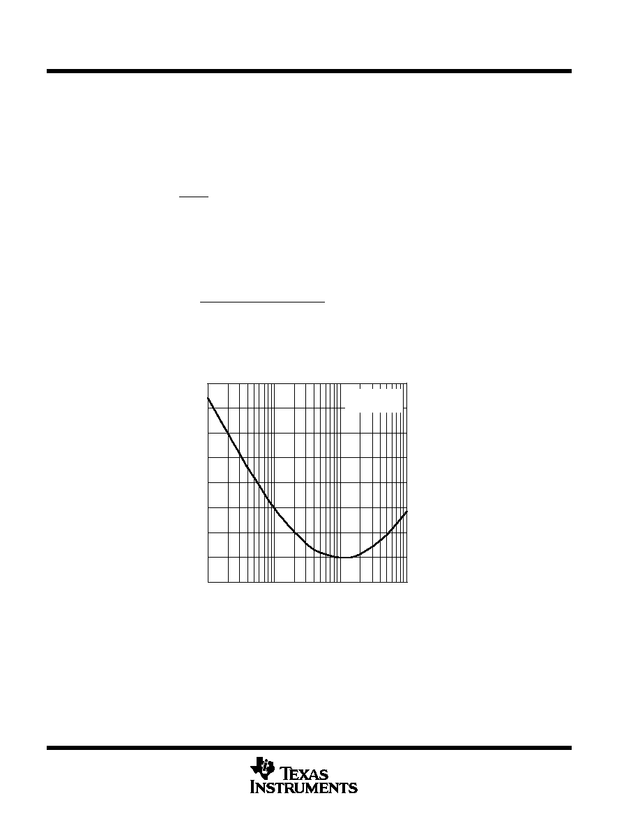
The next consideration is the package constraints. The two sources of heat within an amplifier are quiescent
power and output power. The designer should never forget about the quiescent heat generated within the
device, especially multiamplifier devices. Because these devices have linear output stages (Class-AB), most
of the heat dissipation is at low output voltages with high output currents. Figure 45 and Figure 46 show this
effect, along with the quiescent heat, with an ambient air temperature of 50
∞
C. Obviously, as the ambient
temperature increases, the limit lines shown will drop accordingly. The area under each respective limit line is
considered the safe operating area. Any condition above this line will exceed the amplifier's limits and failure
may result. When using V
CC
=
±
6 V, there is generally not a heat problem, even with SOIC packages.
However, when using V
CC
=
±
12 V, the SOIC package is severely limited in the amount of heat it can dissipate.
The other key factor when looking at these graphs is how the devices are mounted on the PCB. The PowerPAD
devices are extremely useful for heat dissipation. But, the device should always be soldered to a copper plane
to fully use the heat dissipation properties of the PowerPAD. The standard SOIC package, on the other hand,
is highly dependent on how it is mounted on the PCB. As more trace and copper area is placed around the
device,
JA
decreases and the heat dissipation capability increases. The currents and voltages shown in these
graphs are for the total package.
Figure 45
10
100
1000
0
1
2
3
4
5
6
Both Channels
TJ = 150
∞
C
TA = 50
∞
C
Maximum Output
Current Limit Line
VCC =
±
6 V
PWP
JA = 37.5
∞
C/W
DDA
JA = 45.8
∞
C/W
SO-14 Package
JA = 67
∞
C/W
High-K Test PCB
SO-8 Package
JA = 95
∞
C/W
High-K Test PCB
≠
Maximum RMS Output Current
≠
mA
MAXIMUM RMS OUTPUT CURRENT
vs
RMS OUTPUT VOLTAGE (DUE TO THERMAL LIMITS)
I O
VO ≠ RMS Output Voltage ≠ V
Figure 46
10
100
1000
0
2
4
6
8
10
12
Both Channels
TJ = 150
∞
C
TA = 50
∞
C
Maximum Output
Current Limit Line
VCC =
±
12 V
PWP
JA = 37.5
∞
C/W
DDA
JA = 45.8
∞
C/W
SO-14 Package
JA = 67
∞
C/W
High-K Test PCB
SO-8 Package
JA = 95
∞
C/W
High-K Test PCB
Safe
Operating
Area
VO ≠ RMS Output Voltage ≠ V
MAXIMUM RMS OUTPUT CURRENT
vs
RMS OUTPUT VOLTAGE (DUE TO THERMAL LIMITS)
≠
Maximum RMS Output Current
≠
mA
I O
THS6042, THS6043
350 mA,
±
12 V ADSL CPE LINE DRIVERS
SLOS264G ≠ MARCH 2000 ≠ REVISED DECEMBER 2001
26
POST OFFICE BOX 655303
∑
DALLAS, TEXAS 75265
APPLICATION INFORMATION
recommended feedback and gain resistor values
As with all current feedback amplifiers, the bandwidth of the THS6042/3 is an inversely proportional function
of the value of the feedback resistor. This can be seen from Figures 1 to 6. The recommended resistors for the
optimum frequency response are shown in Table 1. These should be used as a starting point and once optimum
values are found, 1% tolerance resistors should be used to maintain frequency response characteristics.
Because there is a finite amount of output resistance of the operational amplifier, load resistance can play a
major part in frequency response. This is especially true with these drivers, which tend to drive low-impedance
loads. This can be seen in Figures 1≠6. As the load resistance increases, the output resistance of the amplifier
becomes less dominant at high frequencies. To compensate for this, the feedback resistor may need to be
changed. For most applications, a feedback resistor value of 750
is recommended, which is a good
compromise between bandwidth and phase margin that yields a very stable amplifier.
Table 1. Recommended Feedback (R
f
) Values for Optimum Frequency Response
GAIN
RL = 25
RL = 100
GAIN
VCC =
±
6 V
VCC =
±
12 V
VCC =
±
6 V
VCC =
±
12 V
1
680
560
620
510
2, ≠1
470
430
430
390
4
270
240
270
240
8
200
200
200
200
Consistent with current feedback amplifiers, increasing the gain is best accomplished by changing the gain
resistor, not the feedback resistor. This is because the bandwidth of the amplifier is dominated by the feedback
resistor value and internal dominant-pole capacitor. The ability to control the amplifier gain independently of the
bandwidth constitutes a major advantage of current feedback amplifiers over conventional voltage feedback
amplifiers. Therefore, once a frequency response is found suitable to a particular application, adjust the value
of the gain resistor to increase or decrease the overall amplifier gain.
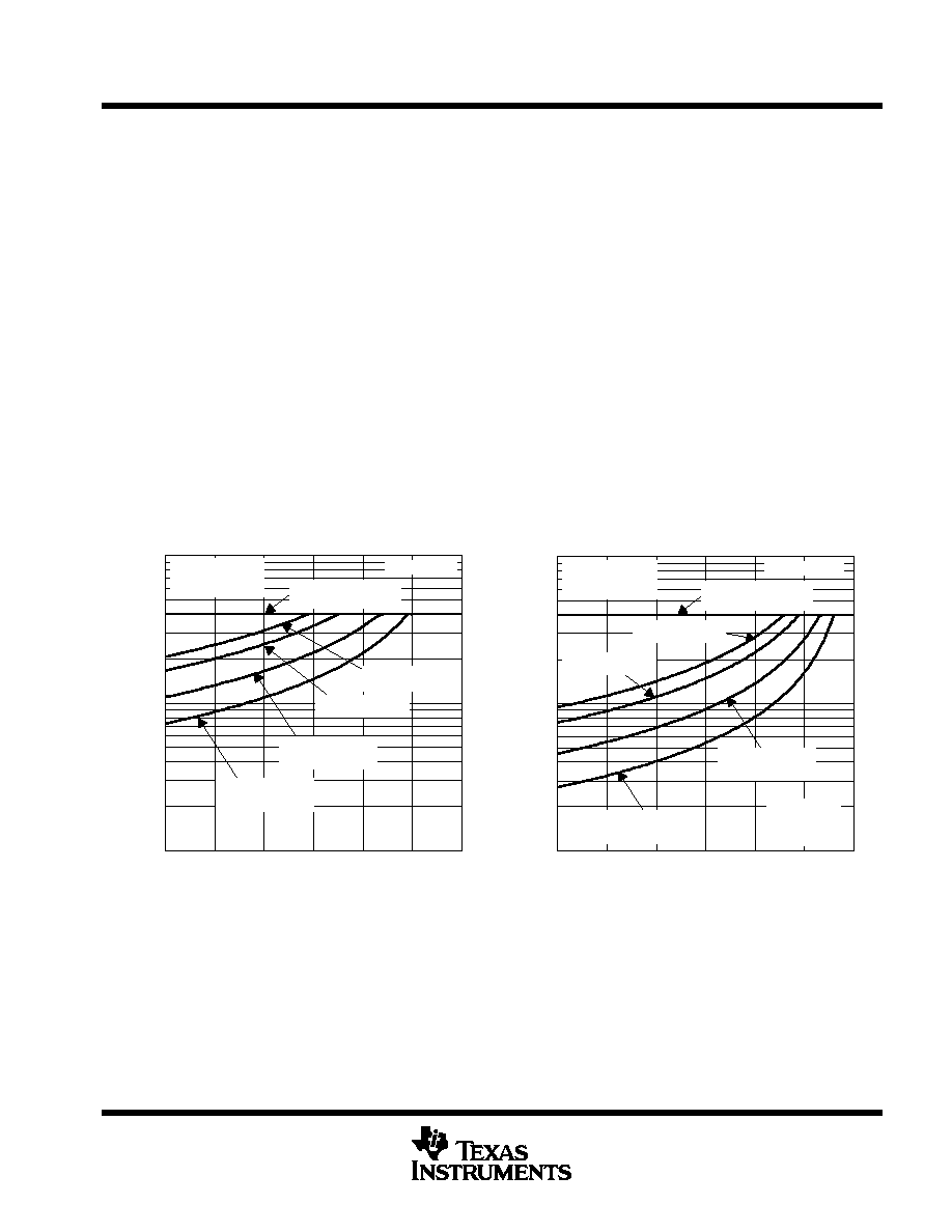
Finally, it is important to realize the effects of the feedback resistance on distortion. Increasing the resistance
decreases the loop gain and may increase the distortion. Decreasing the feedback resistance too low may
increase the bandwidth, but an increase in the load on the output may cause distortion to increase instead of
decreasing. It is also important to know that decreasing load impedance increases total harmonic distortion
(THD). Typically, the third order harmonic distortion increases more than the second order harmonic distortion.
This is illustrated in Figure 10 to 12 and Figures 16 to 18.

THS6042, THS6043
350 mA,
±
12 V ADSL CPE LINE DRIVERS
SLOS264G ≠ MARCH 2000 ≠ REVISED DECEMBER 2001
27
POST OFFICE BOX 655303
∑
DALLAS, TEXAS 75265
APPLICATION INFORMATION
shutdown control
The THS6043 is essentially the same amplifier as the THS6042. The only difference is the added flexibility of
a shutdown circuit. When the shutdown pin signal is low, the THS6043 is active. But, when a shutdown pin is
high (
2 V), the THS6043 is turned off. The shutdown logic is not latched and should always have a signal
applied to it. To help ensure a fixed logic state, an internal 50 k
resistor to GND is utilized. An external resistor,
such as a 3.3 k
, to GND may be added to help improve noise immunity within harsh environments. If no
external resistor is utilized and SHDN pin is left unconnected, the THS6043 defaults to a power-on state. A
simplified circuit can be seen in Figure 47.
+VCC
To Internal
Bias Circuitry
Control
≠VCC
GND
GND
50 k
SHDN
Figure 47. Simplified THS6043 Shutdown Control Circuit
One aspect of the shutdown feature, which is often over-looked, is that the amplifier does not have a large output
impedance while in shutdown mode. This is due to the R
F
and R
G
resistors. This effect is true for any amplifier
connected as an amplifier with gains >1. The internal circuitry may be powered down and in a high-impedance
state, but the resistors are always there. This allows the signal to flow through these resistors and into the ground
connection. Figure 48 shows the results of the output impedance with no feedback resistor and a typically
configured amplifier.
0.01
0.1
1
10
100
1000
10 K
100 K
1 M
10 M
100 M
1 G
Shutdown Mode Impedance
≠
k
f ≠ Frequency ≠ Hz
Open Loop
VCC =
±
5 V to
±
15 V
Gain = ≠8
RF = 750
Figure 48. Output Impedance In Shutdown Mode

THS6042, THS6043
350 mA,
±
12 V ADSL CPE LINE DRIVERS
SLOS264G ≠ MARCH 2000 ≠ REVISED DECEMBER 2001
28
POST OFFICE BOX 655303
∑
DALLAS, TEXAS 75265
APPLICATION INFORMATION
driving a capacitive load
Driving capacitive loads with high performance amplifiers is not a problem as long as certain precautions are
taken. The first is to realize that the THS6042/3 has been internally compensated to maximize its bandwidth
and slew rate performance. When the amplifier is compensated in this manner, capacitive loading directly on
the output decreases the device's phase margin leading to high frequency ringing or oscillations. Therefore, for
capacitive loads of greater than 5 pF, it is recommended that a resistor be placed in series with the output of
the amplifier, as shown in Figure 49. Keep in mind that stray capacitance on the output is also considered
capacitive loading, whether or not it is there on purpose. A minimum value of 5
should work well for most
applications. In ADSL systems, setting the series resistor value to 12.4
both isolates any capacitance loading
and provides the proper line impedance matching at the source end.
+
_
C(Stray) + CL
750
Input
Output
100
12.4
Figure 49. Driving a Capacitive Load
general configurations
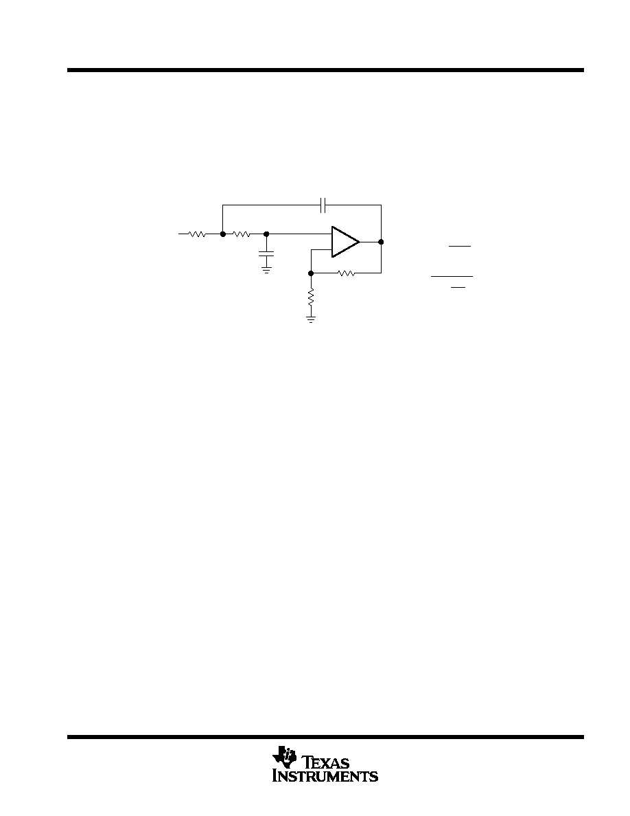
A common error for the first-time CFB user is to create a unity gain buffer amplifier by shorting the output directly
to the inverting input. A CFB amplifier in this configuration oscillates and is not recommended. The THS6042/3,
like all CFB amplifiers, must have a feedback resistor for stable operation. Additionally, placing capacitors
directly from the output to the inverting input is not recommended. This is because, at high frequencies, a
capacitor has a very low impedance. This results in an unstable amplifier and should not be considered when
using a current-feedback amplifier. Because of this, integrators and simple low-pass filters, which are easily
implemented on a VFB amplifier, have to be designed slightly differently. If filtering is required, simply place an
RC-filter at the noninverting terminal of the operational-amplifier (see Figure 50).
VI
VO
C1
+
≠
RG
RF
R1
f
≠3dB
+
1
2
p
R1C1
V
O
V
I
+
1
)
R
F
R
G
1
1
)
sR1C1
Figure 50. Single-Pole Low-Pass Filter
THS6042, THS6043
350 mA,
±
12 V ADSL CPE LINE DRIVERS
SLOS264G ≠ MARCH 2000 ≠ REVISED DECEMBER 2001
29
POST OFFICE BOX 655303
∑
DALLAS, TEXAS 75265
APPLICATION INFORMATION
general configurations (continued)
If a multiple pole filter is required, the use of a Sallen-Key filter can work very well with CFB amplifiers. This is
because the filtering elements are not in the negative feedback loop and stability is not compromised. Because
of their high slew-rates and high bandwidths, CFB amplifiers can create very accurate signals and help minimize
distortion. An example is shown in Figure 51.
VI
C2
R2
R1
C1
RF
RG
R1 = R2 = R
C1 = C2 = C
Q = Peaking Factor
(Butterworth Q = 0.707)
(
=
1
Q
2 ≠
)
RG
RF
_
+
f
≠3dB
+
1
2
p
RC
Figure 51. 2-Pole Low-Pass Sallen-Key Filter
THS6042, THS6043
350 mA,
±
12 V ADSL CPE LINE DRIVERS
SLOS264G ≠ MARCH 2000 ≠ REVISED DECEMBER 2001
30
POST OFFICE BOX 655303
∑
DALLAS, TEXAS 75265
MECHANICAL DATA
D (R-PDSO-G**)
PLASTIC SMALL-OUTLINE PACKAGE
14 PINS SHOWN
4040047 / D 10/96
0.228 (5,80)
0.244 (6,20)
0.069 (1,75) MAX
0.010 (0,25)
0.004 (0,10)
1
14
0.014 (0,35)
0.020 (0,51)
A
0.157 (4,00)
0.150 (3,81)
7
8
0.044 (1,12)
0.016 (0,40)
Seating Plane
0.010 (0,25)
PINS **
0.008 (0,20) NOM
A MIN
A MAX
DIM
Gage Plane
0.189
(4,80)
(5,00)
0.197
8
(8,55)
(8,75)
0.337
14
0.344
(9,80)
16
0.394
(10,00)
0.386
0.004 (0,10)
M
0.010 (0,25)
0.050 (1,27)
0
∞
≠ 8
∞
NOTES: A. All linear dimensions are in inches (millimeters).
B. This drawing is subject to change without notice.
C. Body dimensions do not include mold flash or protrusion, not to exceed 0.006 (0,15).
D. Falls within JEDEC MS-012
THS6042, THS6043
350 mA,
±
12 V ADSL CPE LINE DRIVERS
SLOS264G ≠ MARCH 2000 ≠ REVISED DECEMBER 2001
31
POST OFFICE BOX 655303
∑
DALLAS, TEXAS 75265
MECHANICAL DATA
DDA (S≠PDSO≠G8)
Power PAD
t
PLASTIC SMALL-OUTLINE
6,20
5,84
3,81
3,99
4202561/A 02/01
8
5
1
4
1,68 MAX
0,13
4,98
4,80
0
∞
≠8
∞
0,41
0,89
0,25
0,20 NOM
Seating Plane
0,49
0,35
0,03
1,40
1,55
Thermal Pad
(See Note D)
M
0,10
0,10
1,27
Gage Plane
NOTES: A. All linear dimensions are in millimeters.
B. This drawing is subject to change without notice.
C. Body dimensions do not include mold flash or protrusion not to exceed 0,15.
D. The package thermal performance may be enhanced by bonding the thermal pad to an external thermal plane.
This pad is electrically and thermally connected to the backside of the die and possibly selected leads.
PowerPAD is a trademark of Texas Instruments.

THS6042, THS6043
350 mA,
±
12 V ADSL CPE LINE DRIVERS
SLOS264G ≠ MARCH 2000 ≠ REVISED DECEMBER 2001
32
POST OFFICE BOX 655303
∑
DALLAS, TEXAS 75265
MECHANICAL INFORMATION
PWP (R-PDSO-G**)
PowerPAD
PLASTIC SMALL-OUTLINE PACKAGE
4073225/E 03/97
0,50
0,75
0,25
0,15 NOM
Thermal Pad
(See Note D)
Gage Plane
28
24
7,70
7,90
20
6,40
6,60
9,60
9,80
6,60
6,20
11
0,19
4,50
4,30
10
0,15
20
A
1
0,30
1,20 MAX
16
14
5,10
4,90
PINS **
4,90
5,10
DIM
A MIN
A MAX
0,05
Seating Plane
0,65
0,10
M
0,10
0
∞
≠ 8
∞
20-PIN SHOWN
NOTES: A. All linear dimensions are in millimeters.
B. This drawing is subject to change without notice.
C. Body dimensions do not include mold flash or protrusions.
D. The package thermal performance may be enhanced by bonding the thermal pad to an external thermal plane. This pad is electrically
and thermally connected to the backside of the die and possibly selected leads.
E. Falls within JEDEC MO-153
PowerPAD is a trademark of Texas Instruments.

IMPORTANT NOTICE
Texas Instruments Incorporated and its subsidiaries (TI) reserve the right to make corrections, modifications,
enhancements, improvements, and other changes to its products and services at any time and to discontinue
any product or service without notice. Customers should obtain the latest relevant information before placing
orders and should verify that such information is current and complete. All products are sold subject to TI's terms
and conditions of sale supplied at the time of order acknowledgment.
TI warrants performance of its hardware products to the specifications applicable at the time of sale in
accordance with TI's standard warranty. Testing and other quality control techniques are used to the extent TI
deems necessary to support this warranty. Except where mandated by government requirements, testing of all
parameters of each product is not necessarily performed.
TI assumes no liability for applications assistance or customer product design. Customers are responsible for
their products and applications using TI components. To minimize the risks associated with customer products
and applications, customers should provide adequate design and operating safeguards.
TI does not warrant or represent that any license, either express or implied, is granted under any TI patent right,
copyright, mask work right, or other TI intellectual property right relating to any combination, machine, or process
in which TI products or services are used. Information published by TI regarding third≠party products or services
does not constitute a license from TI to use such products or services or a warranty or endorsement thereof.
Use of such information may require a license from a third party under the patents or other intellectual property
of the third party, or a license from TI under the patents or other intellectual property of TI.
Reproduction of information in TI data books or data sheets is permissible only if reproduction is without
alteration and is accompanied by all associated warranties, conditions, limitations, and notices. Reproduction
of this information with alteration is an unfair and deceptive business practice. TI is not responsible or liable for
such altered documentation.
Resale of TI products or services with statements different from or beyond the parameters stated by TI for that
product or service voids all express and any implied warranties for the associated TI product or service and
is an unfair and deceptive business practice. TI is not responsible or liable for any such statements.
Mailing Address:
Texas Instruments
Post Office Box 655303
Dallas, Texas 75265
Copyright
2001, Texas Instruments Incorporated